
PCB & Circuit Design
Create a new electronic design from requirements — or turn an existing prototype into a cleaner, manufacturable PCB package.
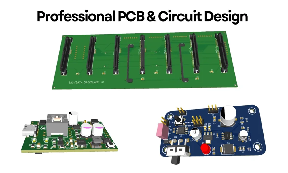
Engineering outputs prepared for the next real step.
Deliverables are scoped around your project rather than forced into a fixed package.
- System architecture and component selection support
- Editable schematic source and PDF export
- PCB layout source files
- Gerber and drill fabrication package
- BOM CSV/XLS and sourcing notes
- CPL/PnP assembly file when required
- 3D STEP model / board preview
- Design notes, wiring and bring-up guidance as scoped
Technical depth where the project needs it.
Schematic engineering
Power trees, MCU interfaces, sensors, communications, protection, programming and test access.
Multilayer layout
Grounding, return paths, power distribution, differential interfaces and high-current routing as required.
Design for manufacture
Footprint checks, assembly constraints, clearances, panel/connector considerations and fabrication outputs.
Production handoff
BOM/CPL consistency, fabrication package review, 3D model and controlled source files.
How this work is approached.
- 01
Define requirements
Voltage, interfaces, dimensions, connectors, environment, cost and manufacturing targets.
- 02
Schematic & review
Architecture is captured into the schematic and checked before expensive layout effort.
- 03
Layout & DFM
Placement, routing, planes, mechanical constraints and production rules are developed.
- 04
Release package
Source, fabrication, assembly and documentation files are exported and cross-checked.
For reverse engineering or third-party hardware, clients are expected to own the hardware or have authorization to analyze, repair or redesign it. Revorix does not accept work intended to violate third-party intellectual-property rights.