
PCB Reverse Engineering
Turn undocumented or unavailable hardware into an editable engineering package for repair, redesign, migration or controlled reproduction.
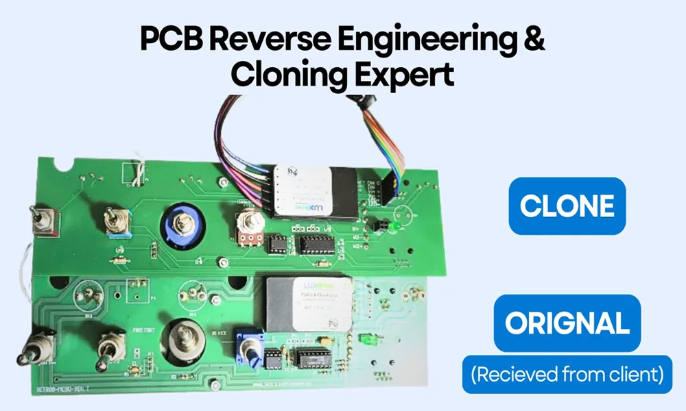
Engineering outputs prepared for the next real step.
Deliverables are scoped around your project rather than forced into a fixed package.
- Reconstructed schematic in editable source format
- Component-level BOM with identification notes
- PCB layout recreation with editable source
- Gerber, drill and manufacturing outputs
- CPL/PnP and assembly data when applicable
- 3D board export and annotated documentation
- Design review for obsolete components and practical substitutions
Technical depth where the project needs it.
Connectivity reconstruction
Trace nets, planes, component relationships and interfaces from physical evidence and available documentation.
Component identification
Identify packages, values, markings and likely function; document uncertainty where evidence is incomplete.
PCB recreation
Rebuild board geometry, placement and routing with manufacturing constraints and mechanical dimensions in mind.
Redesign support
Replace obsolete parts, correct known weaknesses and adapt interfaces while preserving intended function.
How this work is approached.
- 01
Collect evidence
Board photos, measurements, scans, datasheets, working samples and known behavior are reviewed.
- 02
Reconstruct
Connectivity, functions and component relationships are rebuilt into an editable schematic and BOM.
- 03
Recreate & review
PCB geometry and routing are reconstructed, then checked with ERC/DRC and manufacturing rules.
- 04
Validate & hand off
Files are packaged with documentation, open questions and prototype/verification recommendations.
For reverse engineering or third-party hardware, clients are expected to own the hardware or have authorization to analyze, repair or redesign it. Revorix does not accept work intended to violate third-party intellectual-property rights.